Email: Jason.toh@dte-electronics.com
Tel:+65-6844 3612 Fax:+65-6841 1462
Skype: DTE Electronics
Printed Circuit Board
A printed circuit board supports and electrically connects electronic components using conductive tracks, pads and other features etched from copper sheets laminated onto a non-conductive substrate.

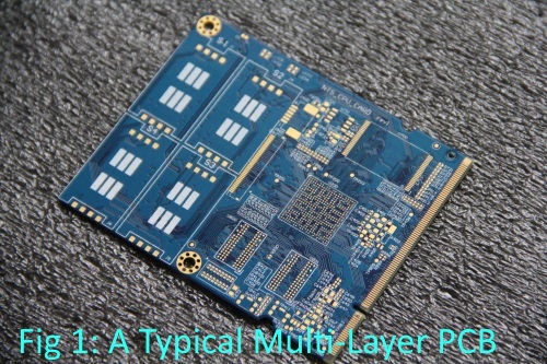
PCBs can be single sided (one copper layer), double sided (two copper layers) or multi-layer (outer and inner layers). Multi-layer PCBs allow for much higher component density. Conductors on different layers are connected with plated-through holes called vias.
PCB Material
FR-4 glass epoxy is the primary insulating substrate upon which the vast majority of rigid PCBs are produced. A thin layer of copper foil is laminated to one or both sides of an FR-4 panel. Circuitry interconnections are etched into copper layers to produce printed circuit boards. Complex circuits are produced in multiple layers. Printed circuit boards are used in all but the simplest electronic products.PCBs require the additional design effort to lay out the circuit, but manufacturing and assembly can be automated. Manufacturing circuits with PCBs is cheaper and faster than with other wiring methods as components are mounted and wired with one single part. Furthermore, operator wiring errors are eliminated.